
Understanding the Electrical Fingerprint of RF Circuits
The Smith Chart looks intimidating: circles and arcs everywhere. But learn a few key ideas and it becomes an easy way to see impedance and how an RF circuit behaves. Whether you're checking a HF antenna, matching a 2-meter power amplifier or looking at a mini-VNA measurement of a filter, it shows things that a table of numbers hides: It's a diagnostic tool as well as a matching tool.
Why the Smith Chart is important
Every RF circuit has an impedance, and it changes with frequency. A sweep might give hundreds of readings. The Smith Chart puts them all on one picture, a map of impedance. Cheap mini-VNAs now let us measure and plot this ourselves with reasonable accuracy.
It helps us to:
Think of the Smith Chart as a map of impedance. With the latest mini-VNA's, we now have powerful equipment at an accessible cost to be able to take measurements and visualise impedance data more easily.
The Five Things to Know
Before exploring more advanced concepts, we should learn these five key things in order to understand the Smith Chart.
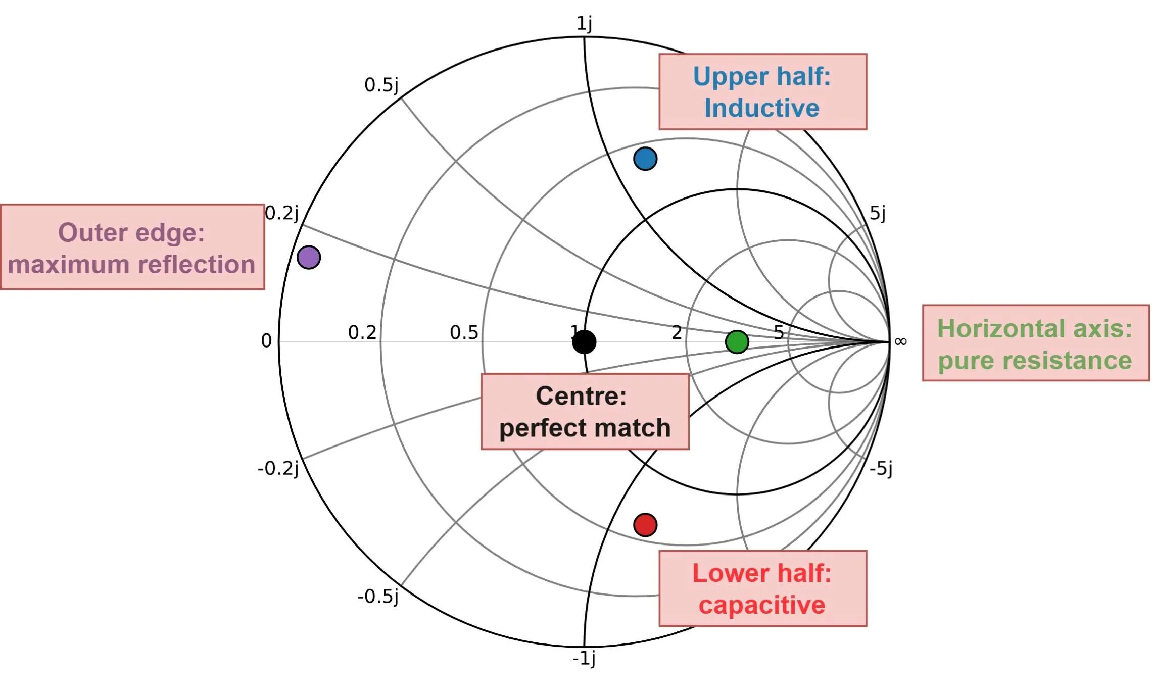
1. The centre is the perfect match
The centre of the chart represents: Z = Z₀ Normally: Z = 50 + j0 Ω
Reflection coefficient is zero, VSWR (voltage standing wave ratio) is 1:1, return loss is at its maximum and power transfer is best. The nearer a point is to the centre, the better the match.
2. The upper half is inductive
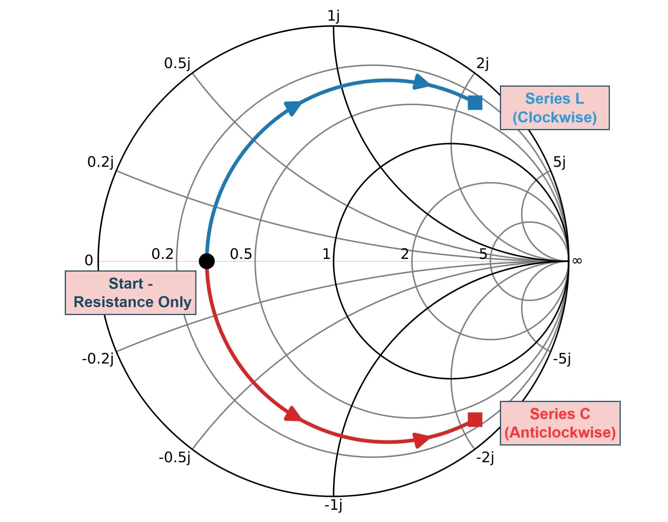
Positive reactance (+jX). Examples: an antenna above resonance, or a coil. To cancel it, add the opposite type of reactance (capacitance).
3. The lower half is capacitive
Negative reactance (−jX). Examples: an antenna below resonance, or a capacitor. To cancel it, add inductance.
4. The horizontal axis is pure resistance
Reactance is zero here. When a trace crosses it, the circuit is resonant. That doesn't mean 50 Ω: a resonant antenna might show 12 Ω, 50 Ω or 120 Ω. Only the centre is both resonant and matched.
5. The outer edge is maximum reflection
Resistance is zero, so the load is purely reactive and almost no power is absorbed. Moving outwards means higher reflection, higher VSWR and a worse match.
Reading a Point on the Smith Chart
Circles that all touch the right-hand edge of the Smith Chart are lines of constant resistance. The circle through the centre is 50 Ω. Arcs that curve up or down from the right-hand edge are lines of constant reactance. Arcs above the axis are inductive, and below are capacitive. Read where the circle and arc meet and you have R + jX.
Moving around the chart
This is the basis of matching:
Reading a Frequency Sweep
One point is the impedance at one frequency. A trace is a sweep across many frequencies. The pattern it draws is the circuit's impedance fingerprint.
Smith Charts and Antennas
Most of us meet the Smith Chart through antenna measurements. It shows:
A trace passing close to the centre means a good match at that frequency. Several crossings of the real axis suggest several resonances, common in dual-band and multi-band antennas.
Reading This Trace: A Worked Example
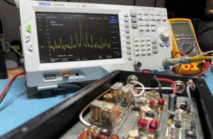
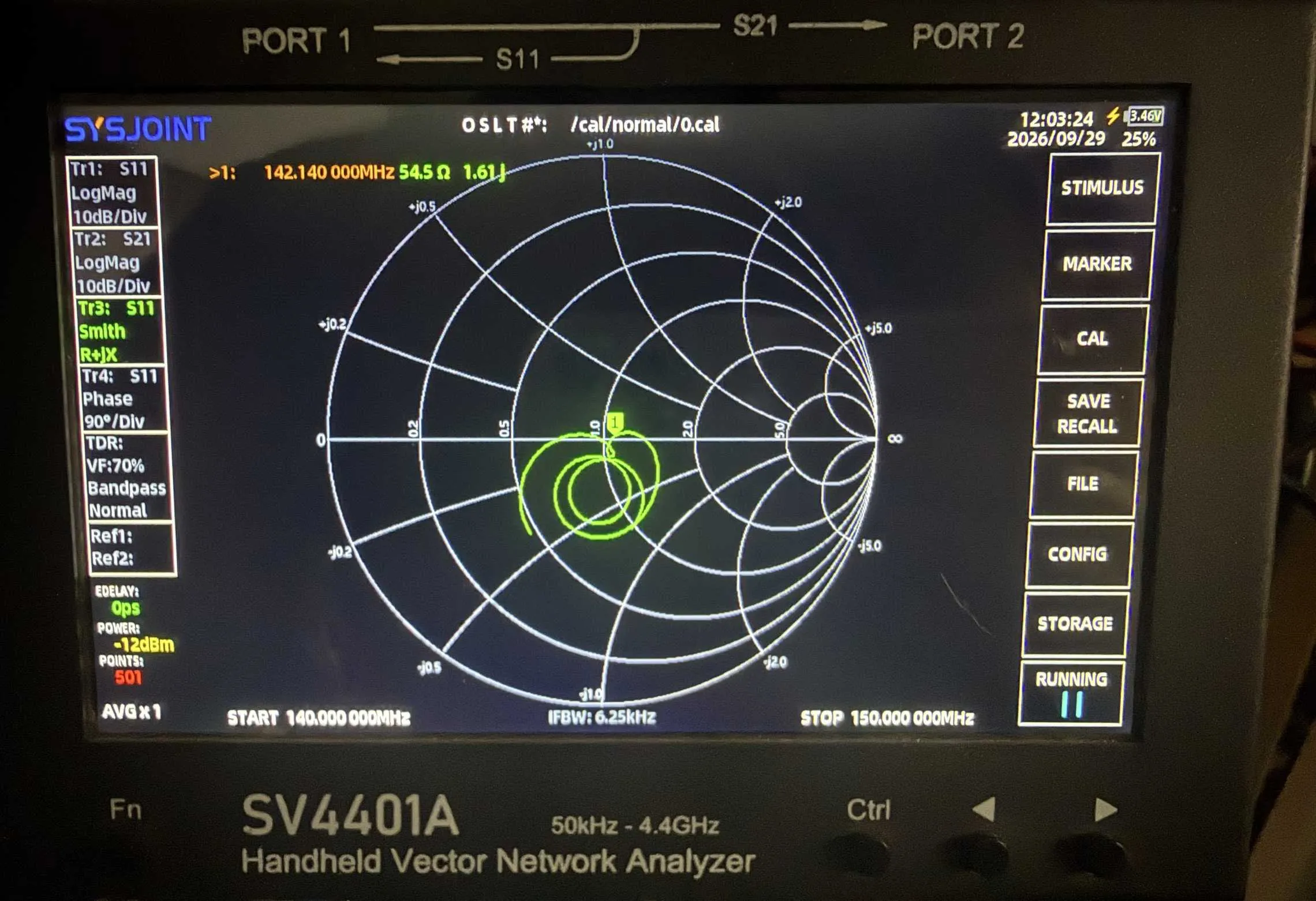
The photo above shows a real sweep of a 144MHz Yagi I was building, using my handheld VNA, across 140–150 MHz.
The marker reading shows the best match is around 142 MHz, so it's a bit low and needs slight adjustment. The trace doesn't sweep smoothly across the chart the way a single resonance usually does. It loops back on itself two or three times, all tightly wound close to the centre. Two things can cause that kind of loop:
1. The antenna has multiple closely-spaced resonant modes: an antenna would need an unusually high Q to sweep round the chart two or three times in just 10 MHz.
2. There's extra electrical line length between the VNA and the antenna that hasn't been compensated for.
In my case, I was measuring the antenna from the shack via a length of coaxial cable. This extra line length was rotating the trace around the chart as the frequency changed but didn't change how close it sat to the centre. Because these loops stay tight and close to the middle across the whole 10 MHz span, the match is pretty good throughout the sweep, not just at the marker.
Smith Charts and Power Amplifiers
For an antenna we want to see its impedance, but for a power transistor we work the other way round: we look at the impedances the transistor needs to see, then we build a matching network to provide them. Note that these are the impedances the network presents to a transistor, not the transistor's own impedance.
Modules and MMICs (monolithic microwave integrated circuits) are already matched to 50 Ω internally. A discrete transistor is not, so it needs matching networks between the device and the external 50 Ω input and output.
A real example: the Ampleon ART1K6FH
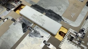
This is a push-pull device (two amplifiers in one package) qualified to 55 V. It's common in commercial amplifiers for HF, 50, 144 and even 432 MHz. Manufacturers rarely publish load-pull data these days, so engineers generate this in simulation software such as Microwave Office or ADS. The values below are simulated for 800 W per side.
Simulated source impedance
50 MHz: 5.88 − j16.03 Ω
70 MHz: 4.06 − j12.53 Ω
144 MHz: 1.70 − j6.60 Ω
432 MHz: 0.81 − j1.52 Ω
Simulated load impedance
50 MHz: 3.71 − j0.41 Ω
70 MHz: 3.46 − j0.56 Ω
144 MHz: 3.27 − j1.00 Ω
432 MHz: 1.58 − j1.00 Ω
These are simulated values for one operating condition, not figures to use in every ART1K6 design. The right impedance depends on frequency, bias, power target, and the reference plane (the point where the impedance is defined, such as the device leads).
ART1K6 - simulated source & load impedances, 800W per side
Before an impedance can be plotted on a conventional Smith Chart, it is normalised to the system impedance. For a 50 Ω system: z = Z ÷ 50
144 MHz load: 3.27 − j1.00 Ω becomes 0.0654 − j0.0200
144 MHz source: 1.70 − j6.60 Ω becomes 0.0340 − j0.1320
Both are very low impedances. They sit right at the left-hand edge of the chart, well away from the 50 Ω centre. Both are slightly capacitive (below the axis), and the source point sits even further below it.
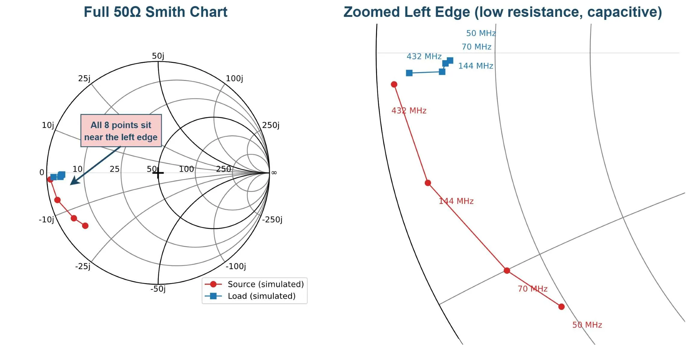
What can we tell from these values already? Points this close to the edge mean a high-Q match, which means narrow bandwidth. High Q is common in high-power amplifiers like this, and is why we would need a separate design for 50, 144 and 432 MHz, rather than one design.
What does the matching network do?
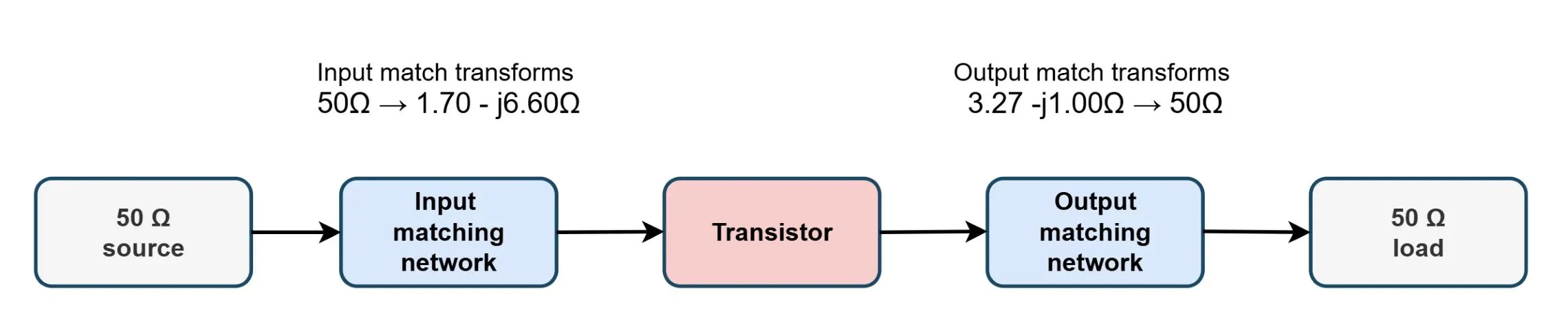
At the input: it transforms the external 50 Ω source to the required source impedance. At 144 MHz that's 1.70 − j6.60 Ω.
At the Output: it transforms the external 50 Ω load to the required load impedance. At 144 MHz that's 3.27 − j1.00 Ω.
On the chart, each network is a path between the centre and the transistor's target point. Real networks use transmission lines, inductors, capacitors, transformers and baluns, often built from miniature coax that acts as balun and transformer in one. The best choice depends on frequency, bandwidth, power, component ratings, PCB construction and acceptable loss.
For an antenna, the centre of the Smith Chart is the goal. For a transistor, 50 Ω at the device is not what gives the best performance. The target is chosen for a design goal such as output power, efficiency, linearity or bandwidth. The aim is not to force the transistor to 50 Ω. It is to transform the external 50 Ω into what the transistor needs to see to deliver this design goal.
Load-pull in brief
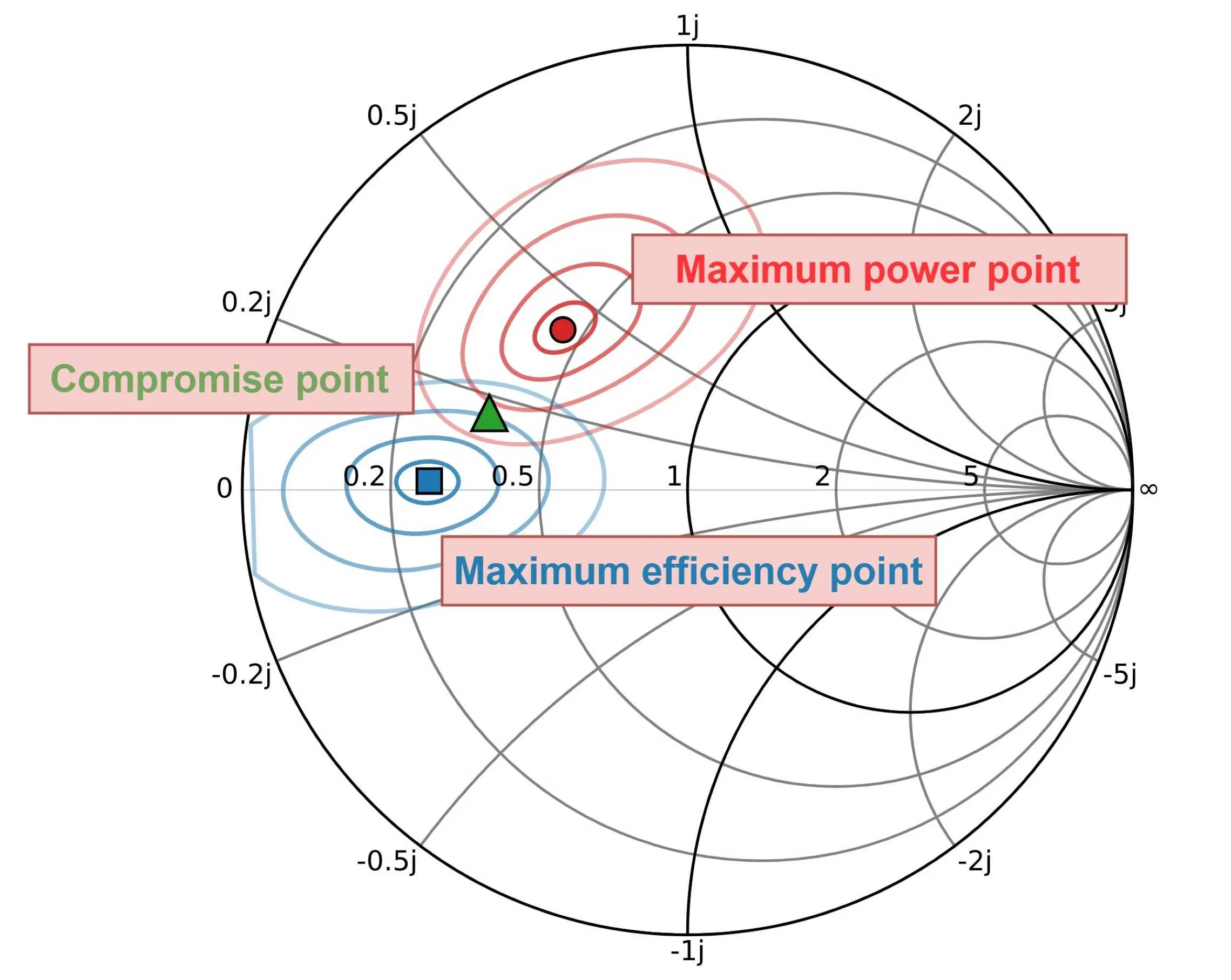
Load-pull tests many impedances and plots contours of constant output power, efficiency, gain or linearity on the chart. The best point for power is usually not the best for efficiency, so designers pick a compromise.
Efficiency matters because waste becomes heat. At 1.6 kW output and 50% drain efficiency, you need 3.2 kW of DC input and must remove 1.6 kW of heat through the package and heatsink.
Impedance changes with frequency
Simulated source resistance falls from 5.88 Ω at 50 MHz to 0.81 Ω at 432 MHz, and source reactance from −j16.03 Ω to −j1.52 Ω. Load impedance moves from 3.71 − j0.41 Ω to 1.58 − j1.00 Ω. A single network cannot follow all of this, so we design a separate amplifier for each band once powers are high and impedances are low.
What the Smith Chart shows us
A table gives the numbers. The Smith Chart shows how they relate to each other.
Limitations
These simulated values are an educational example, not a complete amplifier design. A real design must also consider:
Commercial designers verify with nonlinear simulation. For most amateurs, bench testing and tuning is as far as we can go.