Causes, Identification and Practical Fixes
Oscillation is one of the most common, and most frustrating, causes of instability in RF power-amplifier design. A design that looks perfectly sound on paper can become a self-sustaining oscillator on the bench or after it is fitted into an enclosure. Left unresolved, instability does not merely spoil performance; it can also damage or destroy the active device. This article explains where RF amplifier oscillation comes from, how to identify it and what you can do once you have found it.
Why Do Amplifiers Oscillate?
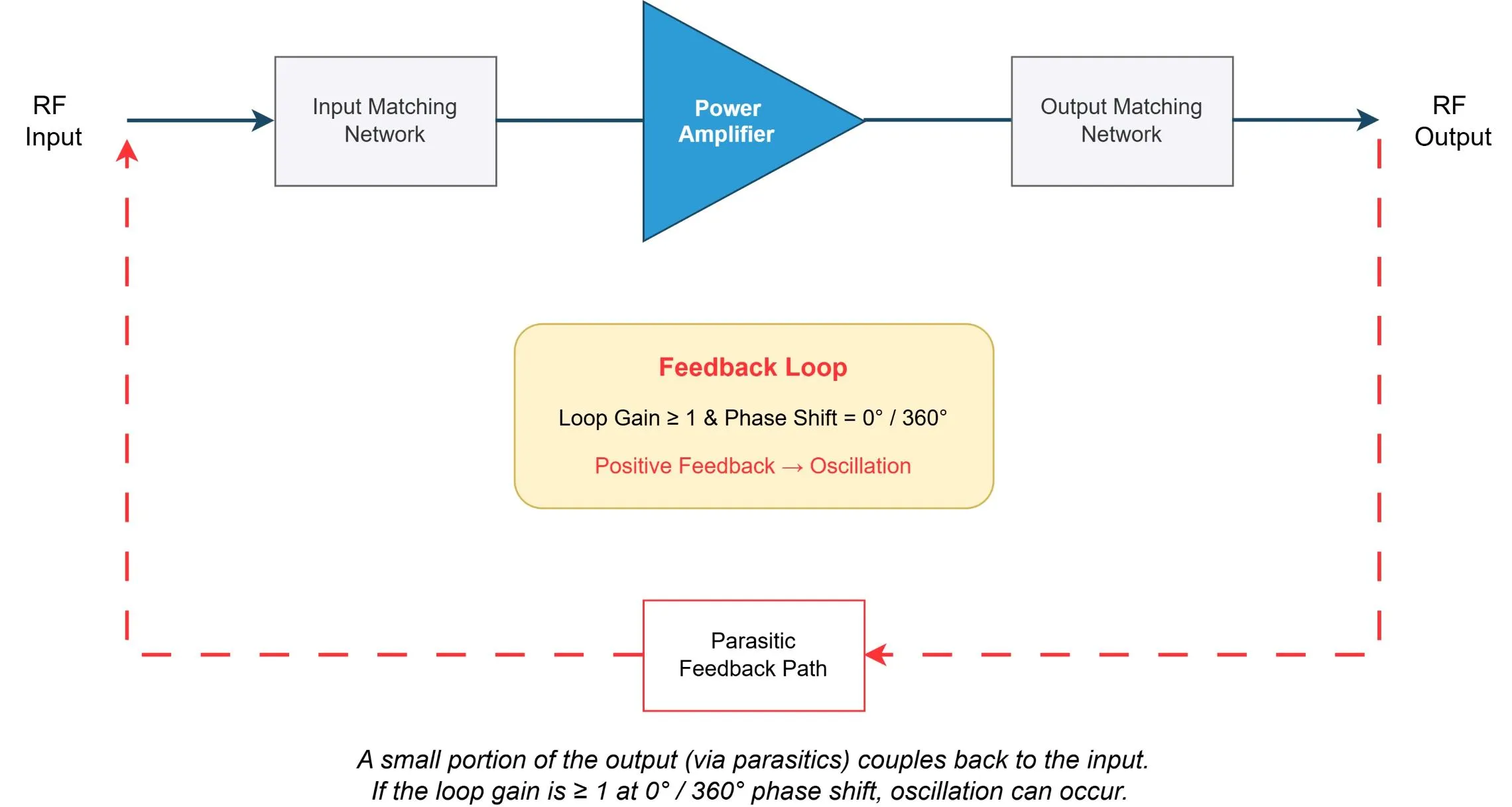
Every amplifier stage has gain, and every physical implementation contains parasitic paths: stray capacitance, inductance, common impedance and electromagnetic coupling can all allow a small proportion of the output signal to return to the input. If the loop gain reaches unity or more at a frequency where the total phase shift satisfies the positive-feedback condition, oscillation can start. Importantly, this does not have to happen at the design frequency. An amplifier may oscillate well below or above its intended operating band, which is why stability must be assessed over a much wider frequency range and across the expected range of bias, drive, temperature and source/load impedance.
Unitended Feedback Loop in an RF Power Amplifier
Root Causes
Negative resistance or insufficient stability margin
At some frequencies and terminations, an active device can present an impedance associated with potential instability. Small-signal S-parameters are extremely useful here: Rollett’s K-factor and |Δ|, the μ stability factors and input/output stability circles can show whether the two-port is unconditionally stable or only conditionally stable for the measured bias condition. However, small-signal data does not describe every large-signal, thermal or bias-network effect, so it should not be the only check.
Positive feedback paths
Poor layout, shared ground or supply impedance, and inadequate isolation between stages can create unintended feedback. Package parasitics, via inductance and coupling through the enclosure can contribute as well. At microwave frequencies, even a physically short path can provide the phase shift needed to close the loop.
Unsuitable component values or behaviour
A bypass or coupling capacitor is not ideal. Its equivalent series inductance and resistance matter, and above its self-resonant frequency it becomes inductive rather than capacitive. A capacitor that looks suitable from its nominal value alone may therefore provide poor decoupling at the frequency that matters. RC feedback and damping networks can also lose effectiveness if their component values, parasitics or placement are wrong.
Power-supply and bias-network problems
Bench supplies, DC-DC converters and bias controllers can introduce noise or unwanted impedance into the supply path. Long leads add inductance and can pick up or radiate interference, while inadequate local decoupling allows RF or low-frequency energy to circulate through the bias network. Use a hierarchy of decoupling values close to the device, with sensible damping where required, and keep current-return paths short.
The smallest-value capacitor (the one with the highest self-resonant frequency) should be placed physically closest to the drain, on the far side of the bias resistor or inductor in a VHF/UHF amplifier. At higher frequencies, a λ/4 track can replace the inductor: it transforms the RF short circuit provided by the capacitor at one end into an open circuit at the other end, which in this case is the drain. Note that the lowest-impedance decoupling path is set by the total series inductance of capacitor, pads, trace and via, not by capacitance alone.
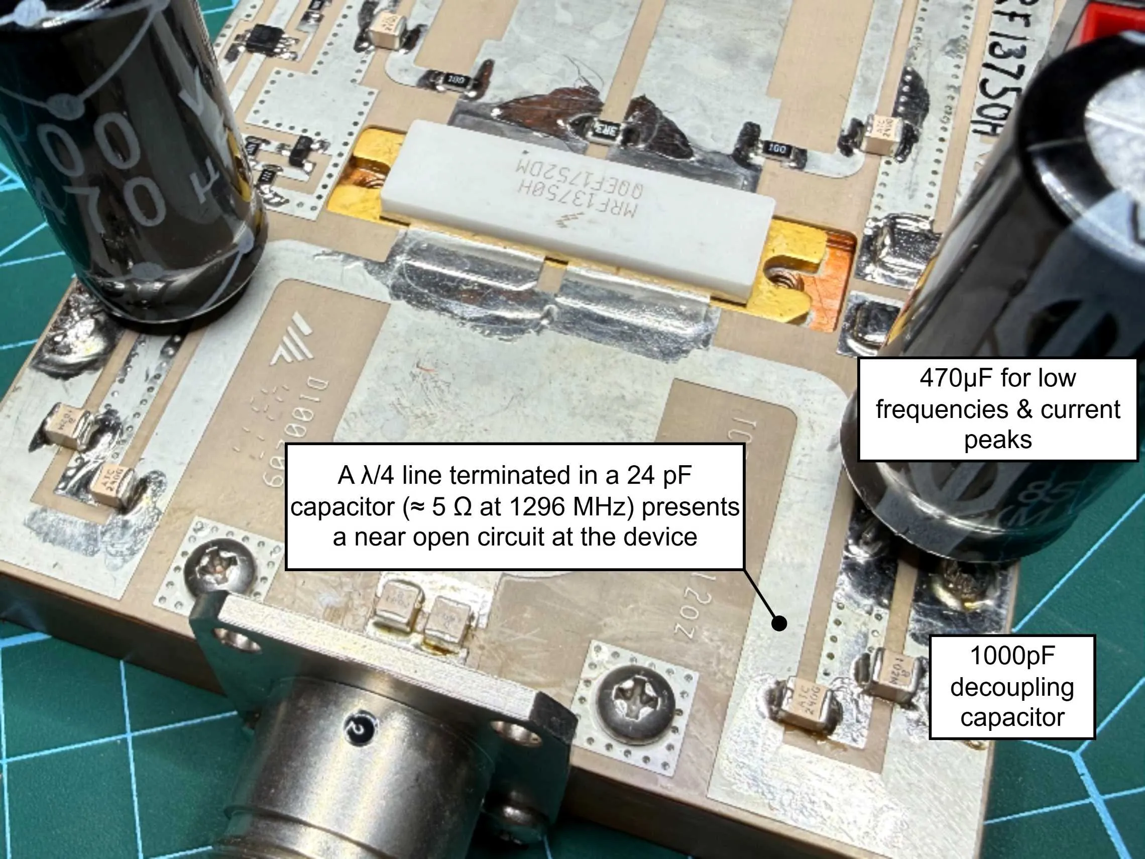
The DC to the Drains on this 1296 MHz LDMOS transistor use a low impedance capacitor at λ/4 distance which translates to a near open at the drain, therefore not harming RF performance. 1000pF and 470µF decouple lower frequencies and provides energy for current delivery during SSB speach peaks.
Supply voltage and bias sequencing also matter. Changing drain or collector voltage alters the device operating point and capacitances. During power-up, power-down or current limiting, the amplifier may briefly pass through a condition that is less stable than its normal steady-state operating point.
Poor RF termination
A mismatched source or load can present an impedance that moves a conditionally stable device into an unstable region. Verify the fixture, cables, connectors, isolators and load with a vector network analyser. For a power amplifier, also consider realistic load mismatch at the intended power level; a passive small-signal measurement alone may not reproduce every large-signal condition.
Cavity and enclosure effects
At higher frequencies, the mechanical cavity around a PA becomes part of the RF environment. Cavity modes, lid coupling and radiation between input and output structures can affect both performance and stability. The enclosure should therefore be included in the electromagnetic assessment rather than treated as an afterthought. RF absorber on the lid can be a useful diagnostic or remedial measure, but correcting the underlying geometry and isolation is preferable where practical.
Feedback in multistage amplifiers
In a chain of gain stages, energy can leak from a later stage back to an earlier one and arrive with the correct phase to form a loop around several stages. Symptoms can include gain suck-outs, unexpected spurs, erratic compression and unexplained changes in current draw.
Identifying Oscillation
A vector network analyser is valuable for measuring match, gain and small-signal stability, and even a Nano VNA can help with this, but a spectrum analyser or oscilloscope is often the most direct way to observe an oscillation in operation. Don't forget to use suitable attenuation, DC blocking and couplers so that the instruments are protected.
Basic procedure
What to look for
Practical bench checks
Fixing Oscillations in Amplifiers
There is no single cure for PA instability. The most reliable approach is to change one thing at a time, repeat the same measurement and keep a record of what moved, disappeared or became worse. Common approaches include:
Worked Example: Compression-Triggered Sidebands
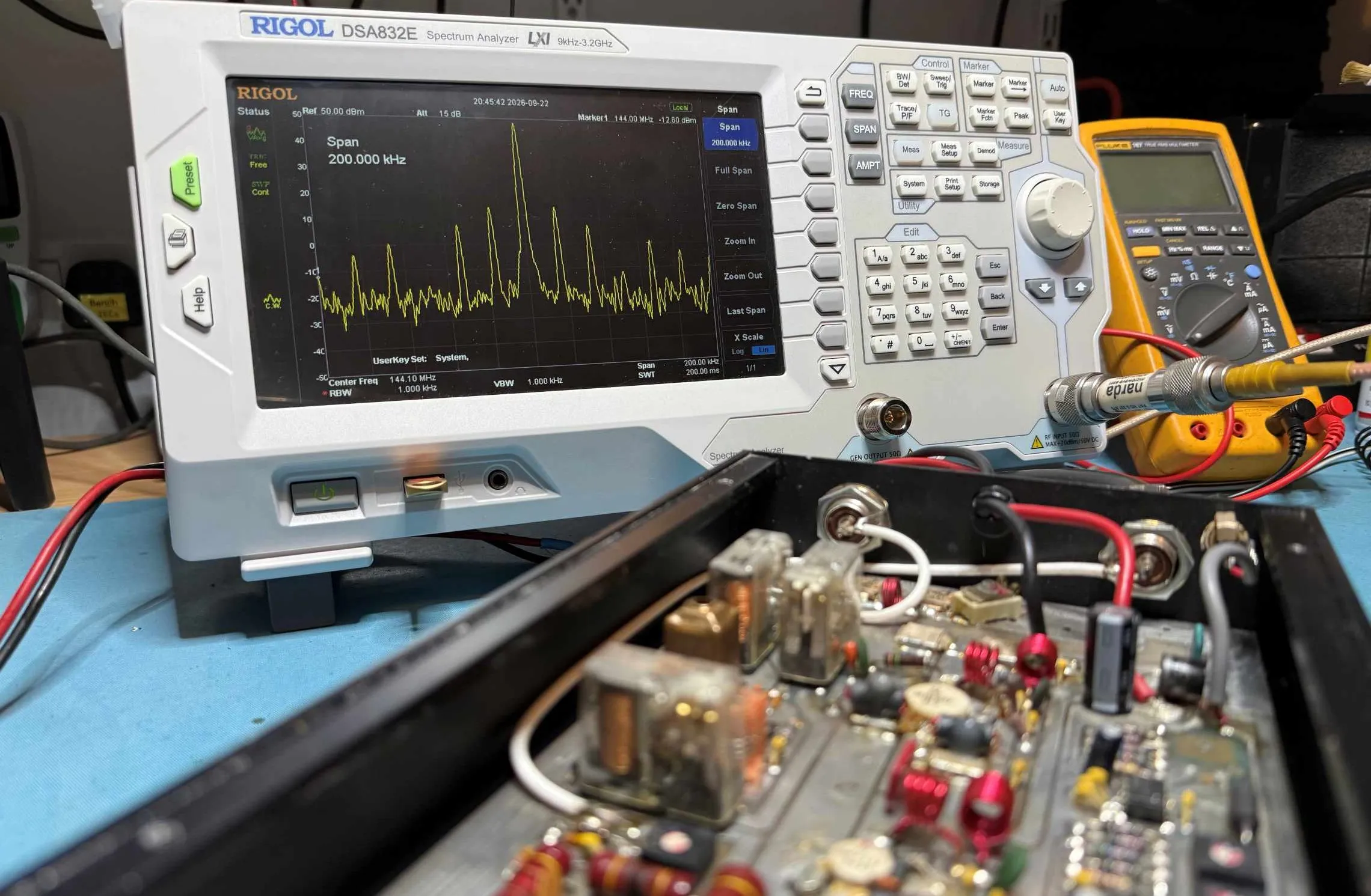
During testing of a 144 MHz amplifier, the output looked clean at low and moderate drive. Once the device was driven into compression, sidebands appeared suddenly at approximately ±17.6 kHz spacing from the carrier, about 33 dB down. The sidebands were absent below the compression point.
This behaviour is consistent with a low-frequency instability or control-loop interaction that modulates the RF carrier once the amplifier is driven hard. Compression changes device current, transconductance, capacitances and the impedances presented to the bias networks. A circuit that is stable under small-signal conditions can therefore become unstable at large signal. The symmetrical sidebands show modulation at 17.6 kHz, but they do not, by themselves, prove where that modulation originates.
A check close to DC at the RF output did not show a discrete 17.6 kHz signal. That is not unexpected: a low-frequency fluctuation in a bias or supply path can amplitude- or phase-modulate the RF carrier without appearing as a directly measurable baseband output at the RF connector. Confirmation requires probing the relevant bias rails or using a current probe or oscilloscope at a safe, suitably decoupled point.
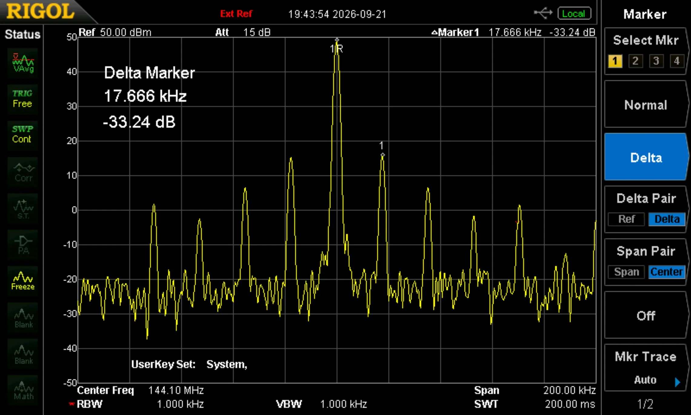
Spectrum analyser display showing marker on 144.1MHz carrier, with a delta marker showing a sideband approximately 17.6KHz away at about -33dBc
Diagnostic steps for this type of case
The result
Adding a low frequency electrolytic decoupling capacitor to the drain supply of the transistor removed the oscillations.
Good Design (techie bit for RF PA Designers)
Assess K, |Δ|, μ/μ′ and stability circles over the widest valid S-parameter range, at relevant bias points and temperatures. Remember that unconditional small-signal stability does not guarantee large-signal stability under compression, mismatch or transients.
Use ADS or Microwave Office or other nonlinear and electromagnetic simulation when the device models are available. Include the package, PCB transitions and enclosure in simulations. Design the grounding, supply return and stage isolation from the outset rather than patching them later.
Select decoupling and damping components from impedance-versus-frequency data and include mounting parasitics. Provide safe RF sampling points and convenient access to bias rails so that the hardware can be diagnosed without improvisation.